Basic Concepts of Printed Circuit Board (PCB)
Printed Circuit Board (PCB) is a circuit board made of ebonite or glass fiber where one side of the surface is coated with thin copper. This type is generally called single side Karana has only one surface that is covered with copper. While the PCB is both sides used for the manufacture of complex circuit, so that both sides can be functioned as wiring pathways, this PCB also serves as a cradle of components. However, it should be with the correct PCB Assembly.
When the circuit is connected to a voltage source, the wiring paths on the PCB will act as a conductor of electrical current. The wiring lines will connect one component with the other components in an integrated manner, so as to form an electronic circuit.
By using PCB in electronic equipment assembly, the following advantages are obtained:
- Easy to find damage, if the tool is interrupted.
- Can be made electronic equipment is getting smaller, Karana where the holder component can be narrowed.
- Little use cable.
- On equipment that works with high frequency can be prevented the occurrence of wild frequency.
There are many providers of PCB assembly service to chosen. You must be smart in choosing the PCB Assembly services.
There are several things to consider in PCB Manufacturing, namely:
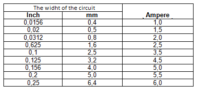
1) The width of the circuit
The good lane width in plotting the PCB path corresponds to the current that will flow on the PCB path.

2) Distance Line
The path distance on the PCB is adjusted to the amount of voltage that will work on the PCB.

3) Eye Size Donut/Pad
In the PCB plan Donut size is two to three times the size of the drill bit to be used.
4) Drill Size
The size of the drill bit used in PCB manufacturing is adjusted to the component to be used.
5) Component Dimension
The dimension of the component or component shape greatly determines the appearance of top and bottom looking arrangement of the PCB to be planned. Similarly, the distance between the legs of a component greatly determines the distance between the donut or pad.
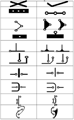
6) Path Form
In planning the PCB is the path to PCB planning and is not recommended for use in PCB planning.
